Ultra-Thin CVD Graphene Thermal Pad: Performance Traps, Interface Challenges and Cost Barriers
Graphene Thermal Pads are often promoted as a revolutionary solution for next-generation thermal management. Leveraging the ultra-high in-plane thermal conductivity of CVD graphene, these ultra-thin thermal pads promise superior performance for high-power chips, 5G devices, and compact electronics. However, real-world applications reveal significant challenges, including high manufacturing costs, interface thermal resistance, and reliability issues during long-term operation. In this article, we explore the scientific basis, engineering limitations, cost barriers, and practical applications of Graphene Thermal Pads, while also comparing them with advanced ceramic thermal interface materials.
At Advanced Ceramics Hub, we specialize in high-quality graphite products, ensuring optimal performance for industrial and scientific applications.
What Is a Graphene Thermal Pad and How Does It Work?
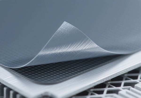
A Graphene Thermal Pad is a heat-conducting sheet based on one or more layers of graphene grown via chemical vapor deposition (CVD). Its primary function is to bridge the microscopic gap between chips and heatsinks, reducing thermal resistance. Unlike polymer-based pads, graphene pads leverage crystalline carbon structure, theoretically enabling thermal conductivities >1500 W/m·K. However, system-level performance depends heavily on interface contact and processing quality.
Key Characteristics of Graphene Thermal Pads:
- Ultra-thin design (few microns to tens of microns)
- High in-plane thermal conductivity (1300–2000 W/m·K)
- Flexibility and lightweight
- Potential integration with polymer or ceramic fillers
Graphene Thermal Pad vs Conventional Pads:
| Parameter | Graphene Thermal Pad | Silicone Pad | Ceramic-Based TIM |
| Thermal Conductivity (W/m·K) | 1300–2000 (theoretical) | 5–10 | 20–200 |
| Thickness (µm) | 5–50 | 200–1000 | 50–300 |
| Flexibility | High | Medium | Low |
| Cost | Very High | Low | Medium |
While graphene thermal pads exhibit record-breaking conductivity, their actual performance depends on interface optimization, unlike ceramic TIMs that offer stable and reproducible results.
Explore our high-quality graphite products.
Why Are Graphene Thermal Pads So Expensive?
The cost of ultra-thin CVD Graphene Thermal Pads is often prohibitive. Production involves high-purity substrates, high-temperature CVD growth (>1000°C), gas purification, and complex transfer processes. Furthermore, low yields (often <60%) push overall cost to unsustainable levels for mass applications.
Cost Breakdown of Graphene Thermal Pads:
| Cost Component | Description | Impact on Price |
| Substrate Material | Copper foil / single-crystal wafer | ★★★★☆ |
| CVD Growth | High energy, vacuum equipment, methane/hydrogen purity | ★★★★★ |
| Transfer Process | Wet/dry transfer, low yield | ★★★★☆ |
| Interface Treatment | Plasma modification, nanoparticle coating | ★★★☆☆ |
| Packaging & Cutting | Ultra-clean environment, precision cutting | ★★★★☆ |
In total, material costs account for ~30% while low yields and complex transfer push final prices up to 5–10× higher than ceramic TIMs.
What Are the Performance Traps of Graphene Thermal Pads?
Despite the exceptional intrinsic conductivity of graphene, actual device-level thermal resistance is often dominated by contact issues. Experimental results show that graphene pads lose >90% of their theoretical thermal advantage when applied between the chip and the heatsink.
Performance Gaps Between Theory and Reality:
| Parameter | Theoretical Value | Measured Value | Reason |
| Thermal Conductivity (W/m·K) | 1300–2000 | 50–100 | Interface resistance |
| Thermal Resistance (cm²·K/W) | 0.0008 | 0.04–0.08 | Poor contact, phonon mismatch |
| Reliability (cycles) | >100,000 | <10,000 | Stress fatigue |
This shows why Graphene Thermal Pads cannot fully replace phase-change or ceramic-based TIMs in high-power chips without major structural innovations.
How Do Interface Challenges Limit Graphene Thermal Pads?
Interface thermal resistance (Rc) is the Achilles’ heel of Graphene Thermal Pads. While bulk graphene is an excellent conductor, the actual heat transfer occurs across imperfect surfaces with micro-voids and roughness. Higher compression can reduce Rc but risks cracking the brittle graphene layer.
Main Interface Challenges:
- Poor surface wetting → limited real contact area
- High contact pressure needed (>1.5 MPa)
- Stress mismatch between graphene and silicon
- Reliability drops under thermal cycling
- Permanent deformation under load
In contrast, ceramic TIMs like AlN or SiC maintain stable contact under similar conditions, offering a more balanced thermal and mechanical performance.
How Do Graphene Thermal Pads Compare to Ceramic Thermal Pads?
While graphene pads promise ultra-thin designs and high intrinsic conductivity, ceramic-based thermal pads (such as AlN, Al₂O₃, BN, SiC) provide more consistent, reliable, and cost-effective solutions. Ceramics are mechanically strong, tolerate compression, and maintain stable performance across thermal cycles.
Graphene vs Ceramic Thermal Pads:
| Property | Graphene Thermal Pad | AlN Thermal Pad | Al₂O₃ Thermal Pad | BN Thermal Pad | SiC Thermal Pad |
| Thermal Conductivity | 1300–2000 (theoretical), 50–100 (effective) | ~170–200 | ~20–30 | ~30–60 | ~120–150 |
| Mechanical Strength | Low (brittle) | High | Very High | Medium | High |
| Reliability (cycling) | Poor | Excellent | Excellent | Good | Excellent |
| Cost | Very High | Medium–High | Low | Medium | Medium–High |
| Best Application | Ultra-thin niche designs | CPUs, LEDs, high-power electronics | General substrates | Microwave/RF systems | Harsh, high-temp devices |
Graphene Thermal Pads are suitable for extreme miniaturization, while ceramics dominate mainstream and industrial electronics due to their balance of thermal conductivity, mechanical robustness, and cost.
Request a custom quote for graphite products.
What Are the Application Areas of Graphene Thermal Pads?
Despite cost and performance traps, Graphene Thermal Pads find niche applications in advanced electronics where ultra-thin design and localized hotspots demand extraordinary solutions.
Key Application Scenarios:
- AI accelerators & GPUs (200–400W chips)
- Foldable smartphones & compact devices
- 5G communication modules
- Aerospace & defense systems
- High-density memory modules
In most cases, Graphene Thermal Pads serve as an experimental or premium material, while ceramic pads dominate mainstream markets.
What Are the Future Trends for Graphene Thermal Pads?
The future of Graphene Thermal Pads lies in hybrid materials and advanced structures. Combining graphene with polymers, ceramics, or liquid metals may balance conductivity with mechanical resilience and reduce costs.
Future Directions in Graphene Thermal Pads:
- Composite pads (Graphene + AlN or BN fillers)
- Direct CVD growth on heatsinks to skip the transfer process
- Surface functionalization for better contact
- AI-driven process optimization for higher yields
- Large-scale roll-to-roll graphene synthesis
Hybrid approaches are expected to bridge the gap between ultra-high conductivity and real-world reliability, making Graphene Thermal Pads more commercially viable.
FAQ
| Question | Answer |
| What is a Graphene Thermal Pad? | A thin thermal interface material made from CVD-grown graphene with high conductivity. |
| Why are Graphene Thermal Pads so expensive? | Complex CVD growth, low yield, and costly transfer steps push prices higher than ceramics. |
| Are Graphene Thermal Pads better than ceramic pads? | Not always — ceramics provide better reliability and cost-efficiency for most cases. |
| What are the main weaknesses of Graphene Thermal Pads? | Interface resistance, brittleness, high cost, and poor long-term reliability. |
| Where are Graphene Thermal Pads used today? | Mainly in niche, high-performance devices like AI chips, smartphones, and aerospace. |
| Can Graphene Thermal Pads replace liquid metal TIMs? | Not yet — liquid metals still outperform graphene in reducing interface resistance. |
| Do Graphene Thermal Pads degrade over time? | Yes, especially under high pressure and thermal cycling. |
| What ceramic materials are alternatives to Graphene Thermal Pads? | AlN, BN, Al₂O₃, and SiC provide stable conductivity and robustness. |
| How thin are Graphene Thermal Pads? | Typically 5–50 microns, much thinner than polymer pads. |
| Will Graphene Thermal Pads become mainstream? | Only if cost, reliability, and interface resistance challenges are solved. |
Conclusion
Graphene Thermal Pads represent an exciting but problematic frontier in thermal interface materials. While their ultra-thin form factor and record-high intrinsic conductivity make them attractive, real-world limitations—including extreme cost, interface resistance, and brittle nature—prevent large-scale adoption. Ceramic thermal pads, despite lower conductivity, remain dominant in the market due to their balance of performance, reliability, and cost-effectiveness. The future likely lies in hybrid approaches that combine the best of graphene and ceramics, supported by innovations in processing and structural design.
Looking for high-quality graphite products? Contact us today!