Top 10 Advanced Ceramic Materials of the Future: Breakthroughs & Applications
Advanced ceramics are revolutionizing various fields due to their unique properties, including high-temperature resistance, electrical insulation, high mechanical strength, and specialized functionalities such as piezoelectricity. As industries push the boundaries of technology, the demand for more specialized and high-performance materials has increased. In this blog post, we will explore the top 10 advanced ceramic materials that are likely to shape the future of multiple industries, from electronics to medicine, aerospace to renewable energy. These materials represent the cutting edge of materials science and have promising applications that are already impacting today’s technology.
At Advanced Ceramics Hub, we specialize in high-quality advanced ceramic products, utilizing a diverse range of materials and specifications to ensure optimal performance for industrial and scientific applications.
What Are Advanced Ceramics?
Advanced ceramics, also known as technical ceramics, engineered ceramics, or high-performance ceramics, are a class of ceramic materials designed to exhibit superior mechanical, thermal, electrical, or chemical properties compared to traditional ceramics. They are typically made from highly refined raw materials (such as oxides, carbides, nitrides, or borides) and are engineered for specific applications requiring extreme durability, heat resistance, or electrical performance.
Key Characteristics of Advanced Ceramics:
- High Strength & Hardness – Resistant to wear, abrasion, and deformation (e.g., silicon carbide, alumina).
- Heat Resistance – Can withstand extreme temperatures (e.g., zirconia, silicon nitride in jet engines).
- Corrosion Resistance – Inert to chemicals, acids, and harsh environments (e.g., alumina in chemical processing).
- Electrical Properties – Can be insulators (alumina), semiconductors (silicon carbide), or superconductors (certain oxides).
- Biocompatibility – Used in medical implants (e.g., zirconia in dental crowns).
- Low Density – Lighter than metals, making them ideal for aerospace applications.
Common Types of Advanced Ceramics:
- Oxide Ceramics (Alumina, Zirconia) – Used in medical, cutting tools, and insulators.
- Non-Oxide Ceramics (Silicon Carbide, Silicon Nitride) – High-temperature applications like turbine blades.
- Composite Ceramics – Reinforced for enhanced toughness (e.g., Alumina-Titanium composites).
Key Applications of Advanced Ceramics:
- Aerospace: Heat shields, turbine blades.
- Automotive: Catalytic converters, brake discs.
- Electronics: Insulators, semiconductors, sensors.
- Medical: Hip implants, dental prosthetics.
- Industrial: Cutting tools, wear-resistant coatings.
Looking for top-quality ceramic products? Explore the Advanced Ceramics Hub’s selection.
Ceramic materials are undergoing a revolutionary transition from traditional manufacturing to smart materials, evolving from an industrial support role to a core driver of technological innovation. With the explosive growth of strategic industries such as new energy, artificial intelligence, and biomedicine, the performance advantages of ceramic materials are continuously being unleashed across multidimensional application scenarios, creating a new industry ecosystem of cross-sector integration. The following provides an in-depth analysis of ten types of pioneering ceramic materials leading industrial transformation and their strategic value.
1. Multilayer Ceramic Capacitors (MLCC)
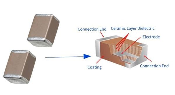
Multilayer Ceramic Capacitors (MLCCs) are a type of compact, high-performance capacitor widely used in modern electronics. They consist of multiple layers of ceramic dielectric material sandwiched between alternating metal electrode layers, all co-fired into a single monolithic structure. MLCCs are valued for their small size, high capacitance, reliability, and excellent high-frequency performance.
Dielectric Materials & Classifications
MLCCs use different ceramic dielectrics, categorized by their temperature stability and capacitance change:
| Class | Material (Example) | Temp. Stability | Capacitance Change | Typical Applications |
| Class I (NP0/C0G) | TiO₂, MgTiO₃ | Ultra-stable (±30 ppm/°C) | Minimal | RF filters, oscillators, precision circuits |
| Class II (X7R, X5R) | BaTiO₃ (Barium Titanate) | Moderate (±15% over range) | Moderate | Decoupling, power supplies, general-purpose |
| Class III (Y5V, Z5U) | BaTiO₃ with additives | Poor (+22%/-82% possible) | High variance | Consumer electronics (non-critical) |
Key Features of MLCCs
- High Capacitance in Small Size – Achieved by stacking many thin dielectric layers (sometimes hundreds).
- Low ESR & ESL – Excellent for high-frequency and fast-switching circuits.
- Wide Range of Capacitance Values – From pF (picofarads) to μF (microfarads).
- Voltage Ratings – From a few volts to kV-range for specialized applications.
- Temperature Stability – Different dielectric classes (e.g., NP0/C0G, X7R, Y5V) offer varying stability.
- Surface-Mount (SMD) Design – Compatible with automated PCB assembly.
Applications of MLCCs
MLCCs are essential in nearly all electronic devices:
- Consumer Electronics (Smartphones, laptops, TVs) – Decoupling, filtering.
- Automotive Electronics – Engine control units (ECUs), ADAS, infotainment.
- Power Supplies – Noise suppression, smoothing.
- RF & Telecom – Signal coupling, impedance matching.
- Medical Devices – Miniaturized implantable and diagnostic equipment.
As the “cell-level” component of modern electronic industry, MLCCs account for 93% of the global ceramic capacitor market, with an annual demand exceeding 4.5 trillion units. Driven by the needs of electric power systems in new energy vehicles (over 10,000 units per vehicle), 5G base stations (up to 15,000 units per station), and AI servers, high-end MLCCs are evolving towards ultra-miniaturization (0201, 0.25×0.125mm), high stacking (over 200 layers), and automotive-grade high reliability (operating temperature range from -55℃ to 150℃).
2. Microwave Dielectric Ceramics
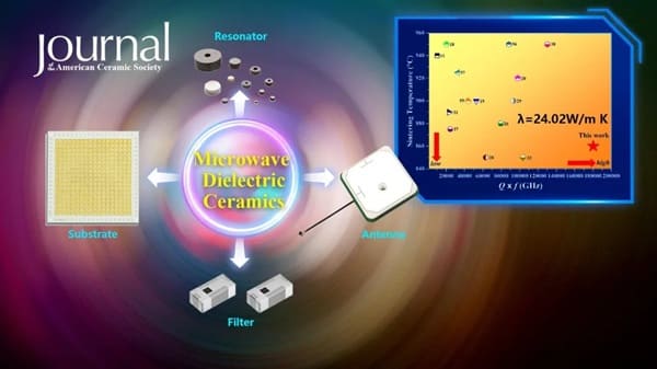
Microwave dielectric ceramics are specialized ceramic materials engineered to exhibit precise dielectric properties at microwave frequencies (typically 300 MHz to 300 GHz). These ceramics are crucial in wireless communication, satellite systems, radar, and 5G/6G technologies due to their ability to efficiently store, transmit, and manipulate electromagnetic waves.
Common Microwave Dielectric Ceramic Materials
Different materials are chosen based on frequency and application requirements:
| Material System | εᵣ (Dielectric Constant) | Q×f (GHz) | τf (ppm/°C) | Applications |
| Alumina (Al₂O₃) | ~9–10 | 300,000–500,000 | -60 to -70 | Substrates, waveguide components |
| Silicon Nitride (Si₃N₄) | ~7–8 | 200,000–400,000 | +30 to +40 | High-power RF applications |
| Barium Titanate (BaTiO₃-based) | ~30–90 | 5,000–50,000 | +100 to +300 | Filters, antennas (adjustable εᵣ) |
| MgTiO₃-CaTiO₃ | ~20–21 | 60,000–80,000 | ±0 (tuned) | GPS, satellite communications |
| Ba(Zn₁/₃Ta₂/₃)O₃ (BZT) | ~28–30 | 100,000–300,000 | ~0 | 5G base stations, radar |
| Li₂MgTiO₄ | ~15–17 | 80,000–120,000 | -30 to -50 | LTCC (Low-Temp Co-fired Ceramics) |
Key Properties of Microwave Dielectric Ceramics
For optimal performance in microwave applications, these ceramics must meet three critical parameters:
✅High Dielectric Constant (εᵣ or Dk)
- Affects the wavelength shortening effect; higher εr allows for miniaturization of components.
- Typical range: εᵣ = 5–120 (e.g., Al₂O₃: ~9, BaTiO₃-based: ~80).
✅Low Dielectric Loss (tan δ or Q×f)
- Minimizes energy dissipation as heat; critical for high-frequency efficiency.
- Measured as Quality Factor (Q = 1/tan δ); higher Q = lower loss.
- Example: Single-crystal Al₂O₃ (Sapphire) has Q×f > 1,000,000 GHz.
✅Near-Zero Temperature Coefficient of Resonant Frequency (τf)
- Ensures stable performance across temperature variations.
- Ideally, τf ≈ 0 ppm/°C (e.g., Ba(Mg₁/₃Ta₂/₃)O₃ has τf ~ 0).
Applications in Modern Technology
✅5G/6G Communication
- Base station filters, antennas, and resonators require low-loss ceramics (e.g., BZT, MgTiO₃).
- Millimeter-wave (mmWave) devices demand ultra-low tan δ materials.
✅Satellite & Radar Systems
- Waveguides, dielectric resonator antennas (DRAs) use Al₂O₃ or Si₃N₄ for high power handling.
✅Consumer Electronics
- Smartphone RF filters, WiFi modules (e.g., LTCC-based multilayer components).
✅Automotive Radar (77 GHz ADAS)
- High-frequency radars require ceramics with stable εᵣ and low loss.
✅LTCC (Low-Temperature Co-fired Ceramics)
- Used in integrated RF modules (combining resistors, capacitors, and inductors).
Microwave dielectric ceramics are the core materials for 5G/6G communication, including dielectric loss (tanδ < 0.001) and the temperature stability of the dielectric constant, which determines the performance of base station filters. The application of millimeter-wave frequencies (28/39GHz) is driving the development of ultra-low dielectric constant ceramics (ε_r = 6-10). Aluminum nitride-based composite materials (ε_r = 8.8, Q×f = 60,000GHz) have become a key technology reserve for 6G.
3. Silicon Nitride Ceramics (Si3N4)
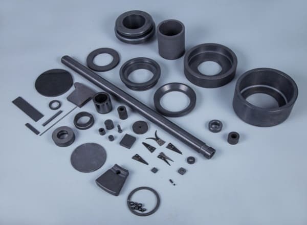
Silicon nitride (Si₃N₄) is one of the most important advanced structural ceramics, known for its exceptional mechanical strength, thermal shock resistance, and chemical stability. It is widely used in extreme environments, such as aerospace, automotive, and biomedical applications.
Key Properties of Silicon Nitride (Si₃N₄)
| Property | Value / Characteristics | Significance |
| Density | 3.1–3.3 g/cm³ | Lighter than steel (~7.8 g/cm³) |
| Hardness (Vickers) | 15–18 GPa | Comparable to alumina, but tougher |
| Flexural Strength | 600–1200 MPa | Higher than most ceramics |
| Fracture Toughness (KIC) | 6–9 MPa·√m | Exceptional for a ceramic (prevents crack propagation) |
| Thermal Conductivity | 15–30 W/m·K | Good heat dissipation |
| Thermal Expansion (CTE) | 2.5–3.5 × 10⁻⁶ /°C (RT–1000°C) | Low expansion → thermal shock resistance |
| Max. Service Temperature | Up to 1400°C (non-oxidizing) | High-temperature stability |
| Dielectric Constant (εᵣ) | ~7–9 (at 1 MHz) | Useful in RF & electronic applications |
| Chemical Resistance | Resistant to acids, molten metals (Al, Zn), and oxidation | Long-term durability |
Types of Silicon Nitride Ceramics
Si₃N₄ is produced in different forms based on processing methods:
✅Reaction-Bonded Silicon Nitride (RBSN)
Made by nitriding silicon powder at ~1200–1400°C.
- Pros: Low shrinkage, near-net shaping.
- Cons: Porosity (~15–20%), lower strength.
- Applications: Lightweight structural parts, crucibles.
✅Hot-Pressed Silicon Nitride (HPSN)
Sintered under high pressure (~20–40 MPa) and temperature (~1700–1800°C).
- Pros: Fully dense, high strength.
- Cons: Limited to simple shapes (due to pressing).
- Applications: Cutting tools, bearings.
✅Sintered Silicon Nitride (SSN)
Pressureless sintering with additives (Y₂O₃, Al₂O₃) at ~1700–1900°C.
- Pros: Complex shapes are possible, and good mechanical properties.
- Cons: Requires sintering aids.
- Applications: Turbine blades, automotive parts.
✅Gas-Pressure Sintered Silicon Nitride (GPSN)
Uses nitrogen gas pressure to enhance densification.
- Pros: Superior mechanical properties.
- Applications: High-performance engine components.
Silicon Nitride (Si3N4) is the core packaging material for the third-generation semiconductor revolution, with a thermal conductivity of 90W/m·K, which perfectly matches silicon chips, while its bending strength (1000MPa) is three times that of aluminum oxide ceramics. In the field of electric motor bearings for new energy vehicles, its penetration rate exceeds 60%, and the 800V high-voltage platform is driving the demand for higher reliability (with rolling contact fatigue life > 1×10^8 cycles).
4. Aluminum Nitride (AlN) Substrates
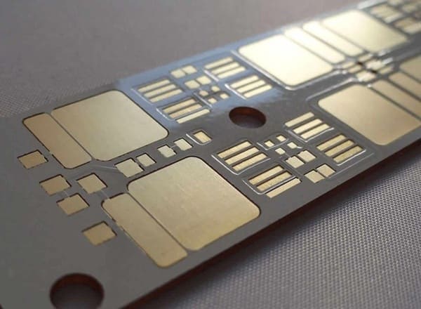
Aluminum Nitride (AlN) is a critical ceramic material used primarily as a substrate in high-power electronics, LED packaging, and RF/microwave applications. It offers an exceptional combination of high thermal conductivity, electrical insulation, and thermal expansion, matching with semiconductors like silicon (Si) and gallium arsenide (GaAs).
Key Properties of AlN Substrates
| Property | Value | Significance |
| Thermal Conductivity (κ) | 170–220 W/m·K (theoretical: 320) | Near that of beryllia (BeO) but non-toxic |
| Dielectric Constant (εᵣ) | ~8.6 (1 MHz) | Low signal delay in high-frequency circuits |
| Dielectric Loss (tan δ) | <0.001 (at 1 MHz) | Minimal energy loss in RF applications |
| CTE (Coeff. Thermal Expansion) | Near that of beryllia (BeO), but non-toxic | Matches Si (3.5) and GaAs (5.8), reducing thermal stress |
| Breakdown Voltage | >15 kV/mm | Excellent electrical insulation |
| Flexural Strength | 300–400 MPa | Mechanically robust for thin substrates |
| Density | 3.26 g/cm³ | Lightweight compared to metals |
| Max. Operating Temp. | Up to 1000°C (in inert) | Stable in high-power environments |
Comparison with Common Substrate Materials
| Material | Thermal Conductivity (W/m·K) | CTE (×10⁻⁶/°C) | Dielectric Constant (εᵣ) | Key Limitations |
| AlN | 170–220 | 4.5 | 8.6 | Higher cost than Al₂O₃ |
| Alumina (Al₂O₃) | 20–30 | 6.5–8.0 | 9.8 | Poor thermal performance for high-power devices |
| BeO (Beryllia) | 250–300 | 6.5–8.0 | 6.8 | Toxic (hazardous when machined) |
| SiC (Silicon Carbide) | 120–490 (varies) | 4.0–4.5 | 40 | Electrically conductive (not for insulation) |
| BN (Boron Nitride) | 50–600 (anisotropic) | 0.6–4.0 | 4.0–5.0 | Lower mechanical strength |
Advantages of AlN Substrates
✔ Best thermal conductivity among non-toxic ceramics (superior to Al₂O₃).
✔ Low dielectric constant & loss → ideal for high-frequency (5G, RF) circuits.
✔ CTE matches semiconductors (Si, GaAs, GaN) → reduces thermal stress in power modules.
✔ Excellent electrical insulation → prevents leakage in high-voltage devices.
Aluminum Nitride (AlN) substrate is a revolutionary material for power electronics heat dissipation, with a thermal conductivity of 170-230W/m·K, which is 10 times that of aluminum oxide, and a thermal expansion coefficient of 4.5ppm/K, perfectly matching SiC chips. The application of this material in new energy vehicle OBC modules is driving the demand for direct-bonded copper (DBC) substrates, with the market size expected to reach $870 million by 2025.
5. Silicon Carbide Fibers (SiC Fibers)
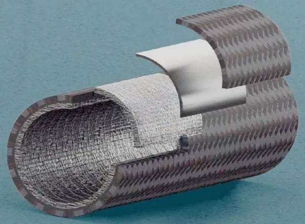
Silicon carbide fibers combine high-temperature stability, tensile strength, and lightweight properties, making them ideal for reinforcing composite materials in aerospace and energy applications. These fibers enhance the performance of ceramic matrix composites (CMCs), which are increasingly replacing metal alloys in jet engines and gas turbines.
Key Properties of SiC Fibers
| Property | Value / Characteristics | Significance |
| Tensile Strength | Outperforms carbon fibers (oxidized>450°C) | Stronger than steel wires |
| Young’s Modulus | 200–450 GPa | High stiffness, resists deformation |
| Density | 2.5–3.0 g/cm³ | Lighter than metals (e.g., Ni superalloys: ~8 g/cm³) |
| Thermal Conductivity | 10–50 W/m·K | Good heat dissipation |
| Max. Operating Temp. | 1200–1600°C (in inert/oxidizing) | Outperforms carbon fibers (oxidize >450°C) |
| Thermal Expansion (CTE) | 3.5–5.0 × 10⁻⁶ /°C | Matches SiC/SiC composites |
| Oxidation Resistance | Excellent (forms protective SiO₂ layer) | Survives harsh environments |
| Chemical Resistance | Resists acids, molten metals (Al, Cu) | Durable in corrosive conditions |
Types of Silicon Carbide (SiC) Fibers
1. First-Generation SiC Fibers (Nicalon™, Tyranno®)
✅Composition: Si-C-O (Oxygen-rich, ~10–15 wt% O)
✅Process: Melt-spinning of polycarbosilane (PCS) + oxidation curing.
✅Limitations:
- Lose strength >1200°C (SiO₂ + C → CO gas).
- Lower thermal conductivity (~10 W/m·K).
2. Second-Generation (Near-Stoichiometric, Hi-Nicalon™, Sylramic®)
✅Composition: SiC with <1% O, excess C or Si.
✅Process: Electron beam curing + pyrolysis.
✅Advantages:
- Higher thermal stability (up to 1400°C).
- Improved thermal conductivity (~30 W/m·K).
3. Third-Generation (Pure SiC, Hi-Nicalon Type S, Tyranno SA)
✅Composition: >99% SiC, almost no oxygen.
✅Process: Chemical vapor deposition (CVD) or advanced polymer pyrolysis.
✅Advantages:
- Best performance (1600°C+ in inert gas).
- Highest thermal conductivity (40–50 W/m·K).
Silicon Carbide (SiC) fibers are critical for ultra-high-temperature applications where metals and carbon fibers fail. Their use in CMCs is revolutionizing aerospace, nuclear, and hypersonic technologies, enabling lighter, more efficient systems. It is widely used as the aerospace super-structural material, with a temperature resistance of up to 1800℃ (500℃ higher than carbon fiber) and a tensile strength of 3.5GPa. CMC composite materials used in aircraft engine combustion chambers can reduce weight by 50% and improve thrust-to-weight ratio by 30%.
6. Ceramic Matrix Diamond Composites
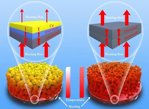
Ceramic Matrix Diamond Composites (CMDCs) are a new class of advanced materials that combine diamond’s extreme thermal conductivity (up to 2000 W/m·K) with the mechanical robustness and oxidation resistance of ceramics (e.g., SiC, AlN). These composites are designed for next-gen thermal management in high-power electronics, aerospace, and defense applications.
Key Properties of CMDCs
| Property | Value | Significance |
| Thermal Conductivity (κ) | 500–1200 W/m·K (vs. Cu: 400) | Best-in-class heat dissipation |
| Coeff. Thermal Expansion (CTE) | 2.5–5.0 × 10⁻⁶ /°C | Matches semiconductors (Si, GaN) |
| Dielectric Constant (εᵣ) | 5–10 (depends on matrix) | Low signal loss in RF applications |
| Breakdown Voltage | >20 kV/mm | Superior electrical insulation |
| Hardness (Vickers) | 30–70 GPa | Near-diamond wear resistance |
| Density | 3.0–4.0 g/cm³ | Lighter than copper (8.96 g/cm³) |
| Max. Operating Temp. | 800–1200°C (in inert) | Stable in extreme environments |
Types of CMDCs
1. Diamond-SiC Composites
- Matrix: Silicon carbide (SiC) + diamond particles/fibers.
- Thermal Conductivity: 600–900 W/m·K.
- Applications: Hypersonic vehicle leading edges, laser diode heat sinks.
2. Diamond-AlN Composites
- Matrix: Aluminum nitride (AlN) + diamond.
- Thermal Conductivity: 700–1200 W/m·K.
- Applications: High-power RF devices, 5G base stations.
3. Diamond-ZrB₂ Composites
- Matrix: Zirconium diboride (ultra-high-temp ceramic).
- Thermal Conductivity: 400–800 W/m·K.
- Applications: Re-entry vehicle thermal protection.
Ceramic Matrix Diamond Composites are applied in an ultimate heat dissipation solution with a thermal conductivity exceeding 600W/m·K (1.5 times that of copper) and a Vickers hardness of 70GPa. In GaN RF device cooling, the interface thermal resistance is reduced to 5mm²·K/W, resulting in a threefold increase in power density.
7. Piezoelectric Ceramics
Piezoelectric ceramics are a class of functional materials that generate an electric charge in response to mechanical stress (direct piezoelectric effect) or undergo mechanical deformation when an electric field is applied (inverse piezoelectric effect). These materials are widely used in sensors, actuators, transducers, and energy harvesting devices.
Key Properties of Piezoelectric Ceramics
| Property | Description |
| Piezoelectric Charge Constant (d₃₃) | Measures charge generated per unit force (pC/N). Higher = more sensitive. |
| Piezoelectric Voltage Constant (g₃₃) | Measures electric field generated per unit stress (mV·m/N). Important for sensors. |
| Electromechanical Coupling Factor (kₜ, kₚ) | Efficiency of energy conversion (0–1). Higher = better actuator/sensor performance. |
| Dielectric Constant (εᵣ) | Affects capacitance and impedance matching. |
| Mechanical Quality Factor (Qₘ) | Indicates vibrational energy loss (higher = lower damping). |
| Curie Temperature (T_c) | Maximum temperature before piezoelectricity is lost. |
Common Piezoelectric Ceramics
| Material | Composition | d₃₃ (pC/N) | Coupling Factor (kₚ/kₜ) | Curie Temp. (T_c, °C) | Key Applications |
| Lead Zirconate Titanate (PZT) | Pb(Zr,Ti)O₃ | 300–600 | 0.6–0.7 (kₚ) | 180–350 | Ultrasonic transducers, fuel injectors |
| Barium Titanate (BaTiO₃) | BaTiO₃ | ~190 | 0.3–0.5 (kₚ) | 120 | Capacitors, low-cost sensors |
| Potassium Sodium Niobate (KNN) | (K, Na)NbO₃ | 200–400 | 0.4–0.5 (kₚ) | 200–300 | Eco-friendly sensors/actuators |
| Bismuth Sodium Titanate (BNT) | (Bi, Na)TiO₃ | 150–300 | 0.4–0.6 (kₚ) | 320 | High-temperature actuators |
| PMN-PT (Relaxor Ferroelectric) | Pb(Mg₁/₃Nb₂/₃)O₃-PbTiO₃ | >2000 | >0.9 (kₜ) | 150–180 | Medical ultrasound, sonar |
Recent developments include
- Lead-Free Alternatives: Environmentally friendly compositions like potassium sodium niobate (KNN).
- High Sensitivity: Improved response for low-force inputs.
- Miniaturization: Thin-film piezoelectrics for wearable devices.
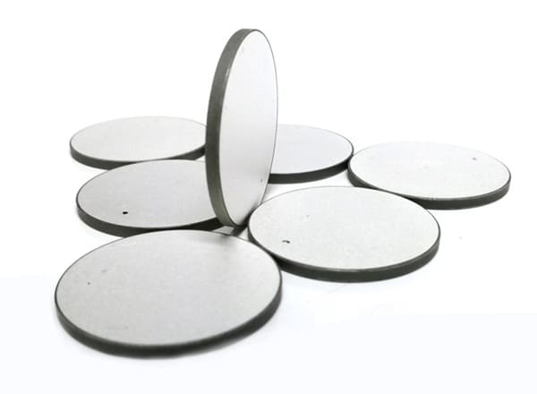
8. Transparent Ceramics
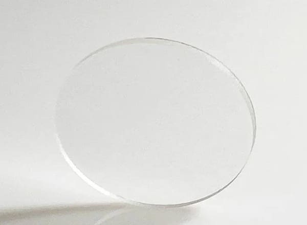
Transparent ceramics are a class of polycrystalline ceramic materials engineered to achieve exceptional optical transparency while maintaining superior mechanical, thermal, and chemical properties compared to traditional glasses and single crystals. These materials are revolutionizing high-performance optical systems, laser technologies, and armor applications.
Key Properties of Transparent Ceramics
| Property | Typical Values | Significance |
| Transmittance | 70-85% (visible to IR) | Comparable to single crystals |
| Refractive Index | 1.7-2.4 | Optical design flexibility |
| Hardness (Vickers) | 10-20 GPa | Scratch-resistant |
| Thermal Conductivity | 5-30 W/m·K | Better than glass |
| Fracture Toughness | 2-5 MPa·m¹/² | More durable than glass |
| Melting Point | 2000-3000°C | High-temp stability |
Common Transparent Ceramics
| Material (Formula) | Common Name | Transmission Range | Key Properties | Primary Applications |
| Aluminum Oxynitride (Al₂₃O₂₇N₅) | ALON | 0.2-5.5 μm | • Vickers Hardness: 18 GPa • Flexural Strength: 300 MPa • Thermal Conductivity: 12 W/m·K | • Transparent armor • IR windows/domes • Sensor protection |
| Magnesium Aluminate Spinel (MgAl₂O₄) | Spinel | 0.2-5.5 μm | • Isotropic cubic structure • Hardness: 15 GPa • Fracture Toughness: 1.4 MPa·m¹/² | • Missile domes • UV/IR optics • High-pressure lamp envelopes |
| Yttrium Aluminum Garnet (Y₃Al₅O₁₂) | YAG | 0.3-5.0 μm | • Excellent laser host • Thermal Conductivity: 14 W/m·K • High damage threshold | • Laser gain media (Nd:YAG) • LED phosphor substrates • Laser windows |
| Polycrystalline Alumina (Al₂O₃) | PCA | 0.4-5.0 μm (semi-transparent) | • Cost-effective • Hardness: 20 GPa • Wear resistant | • Dental restorations • Watch crystals • Substrates |
Innovations include:
- Broadband Transparency: Effective across UV, visible, and IR spectra.
- High Hardness: Up to 9 on the Mohs scale, rivaling sapphire.
- Scalable Production: Cost-effective sintering techniques.
9. 3D-Printed Bioceramics
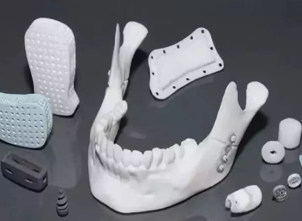
3D-printed bioceramics, such as hydroxyapatite or tricalcium phosphate, represent a transformative advancement in biomedical applications, enabling patient-specific implants with controlled porosity for bone regeneration and tissue engineering. These materials combine biocompatibility with structural customization through additive manufacturing.
Key Characteristics of 3D-Printed Bioceramics
| Property | Importance | Comparison to Traditional Implants |
| Porosity Control | 50-80% adjustable porosity for cell infiltration/vascularization | Superior to machined solid implants |
| Mechanical Strength | Compressive: 2-150 MPa (depends on material/architecture) | Tailorable vs. brittle conventional ceramics |
| Bioactivity | Hydroxyapatite forms bone-like apatite layer | Faster osseointegration than metals |
| Degradation Rate | Weeks to years (tunable via composition) | Resorbable vs. permanent implants |
| Surface Roughness | Ra 5-50 μm (enhances cell attachment) | Better than polished surfaces |
Common 3D-Printed Bioceramic Materials
| Material | Formulation | Key Advantages | Clinical Applications |
| Hydroxyapatite (HAp) | Ca₁₀(PO₄)₆(OH)₂ | • Chemical similarity to bone • Osteoconductive | • Dental/bone grafts • Spinal fusion |
| β-Tricalcium Phosphate (β-TCP) | Ca₃(PO₄)₂ | • Faster resorption than HAp • Supports bone remodeling | • Craniofacial defects • Periodontal repair |
| Biphasic Calcium Phosphate (BCP) | HAp + β-TCP blends | • Balanced resorption/strength • Tunable degradation | • Load-bearing bone voids • Maxillofacial reconstruction |
| Bioactive Glasses | SiO₂-CaO-P₂O₅ systems | • Angiogenic potential • Antibacterial ions (Ag⁺, Ga³⁺) | • Wound healing scaffolds • Infection-resistant implants |
| Zirconia (Y-TZP) | Y₂O₃-stabilized ZrO₂ | • High fracture toughness • Tooth-like aesthetics | • Dental crowns/abutments • Orthopedic bearings |
Advantages Over Conventional Methods
| Feature | 3D-Printed Bioceramics | Traditional Implants |
| Customization | Patient-specific geometry | Limited standard sizes |
| Porosity | Precisely controlled | Often non-porous |
| Production Time | Hours-days (digital workflow) | Weeks (milling/molding) |
| Material Waste | <5% (additive process) | 40-60% (subtractive) |
10. Nanofunctional Ceramics
Nanofunctional ceramics are advanced materials where nanostructuring (1–100 nm scale) enables unprecedented control over mechanical, electrical, thermal, and catalytic properties. These materials leverage quantum effects, high surface area, and interfacial engineering to outperform conventional ceramics.
Key Characteristics of Nanofunctional Ceramics
| Property | Nanoscale Effect | Macroscale Benefit |
| Mechanical Strength | Hall-Petch strengthening (grain boundary effects) | 2–5× higher hardness vs. microcrystalline ceramics |
| Toughness | Nanofibers/platelets deflect cracks | Fracture toughness up to 15 MPa·m¹/² (vs. 3–5 for conventional) |
| Thermal Conductivity | Phonon scattering reduction | Anisotropic κ: 100–400 W/m·K (e.g., nano-SiC) |
| Electrical Properties | Quantum confinement in nanolayers | Tunable bandgap (e.g., transparent conductive ZnO:Al) |
| Catalytic Activity | High surface area (>200 m²/g) | 10–100× more active sites (e.g., nano-TiO₂ photocatalysts) |
Types of Nanofunctional Ceramics
1. Structural Nanoceramics
✅Materials: Nano-Si₃N₄, nano-ZrO₂, Al₂O₃/SiC nanocomposites
✅Features:
- Grain sizes <50 nm → superplasticity at high temps
- Wear-resistant coatings (Vickers hardness 25–35 GPa)
✅Applications:
- Cutting tools with self-sharpening edges
- Jet engine thermal barrier coatings (TBCs)
2. Electroactive Nanoceramics
✅Materials: BaTiO₃ nanoparticles, PZT nanofibers
✅Features:
- Giant permittivity (εᵣ > 20,000 at 1 kHz)
- Flexoelectricity enhanced by strain gradients
✅Applications:
- Microcapacitors for IoT devices
- Nanogenerators for self-powered sensors
3. Energy Nanoceramics
| Material | Function | Application Example |
| LLZO (Li₇La₃Zr₂O₁₂) | Solid-state electrolyte (ionic σ = 10⁻³ S/cm) | All-solid-state batteries |
| Nanoporous SiC | Hydrogen storage (2.5 wt%) | Fuel cell vehicles |
| Nano-LTO (Li₄Ti₅O₁₂) | Ultra-fast anode (100C charging) | Grid-scale energy storage |
Innovations include:
- Nanoparticle Synthesis: Precise control over size and distribution.
- Functional Coatings: Improved performance in sensors and batteries.
- Self-Healing Properties: Emerging designs for durable applications.
Nanofunctional ceramics are the paradigm in materials genome engineering, with ZrO2 nanoceramics achieving a toughness of 15MPa·m^1/2 (five times that of traditional ceramics), and TiO2 nanotubes showing an 80% improvement in photocatalytic efficiency.
Future Trends
Material design is transitioning from trial-and-error based on experience to computational materials science. Manufacturing technology is evolving from micron-level processing to atomic-level manipulation. The application scenarios are advancing from single-function to smart responsiveness. Ceramic materials are redefining the physical boundaries of future technologies, and their depth of innovation will directly determine the height of the next-generation industrial revolution.
For top-quality ceramic products, Advanced Ceramics Hub provides tailored solutions and precision machining techniques for various applications.
Looking for premium ceramic products? Contact us today!