LTCC Technology: A Comprehensive Guide to Applications and Advancements
Low Temperature Co-fired Ceramics (LTCC) is a transformative technology that has revolutionized the electronics industry. It is widely used in various sectors, from telecommunications to automotive and medical devices, due to its unique properties, such as high thermal conductivity, excellent electrical insulation, and the ability to integrate various components on a single substrate. In this guide, we will explore the fundamentals of LTCC technology, its various applications, recent advancements, and challenges. By the end, you will understand why LTCC is a crucial part of modern electronic systems and its role in the development of cutting-edge technologies.
At Advanced Ceramics Hub, we specialize in high-quality ceramic products with a variety of materials and specifications, ensuring optimal performance for industrial and scientific applications.
Understanding LTCC (Low Temperature Co-fired Ceramics) Technology
LTCC refers to a ceramic technology that allows the co-firing of both ceramic and metal materials at relatively low temperatures (typically between 850°C and 1000°C). This low-temperature process helps to preserve the integrity of metal components while creating a robust and reliable substrate for electronic components. The technology involves layering ceramic substrates and conductive materials such as silver, copper, or gold, which are fired together in a kiln to form a solid, integrated component. This process is crucial for creating compact and highly functional electronic devices.
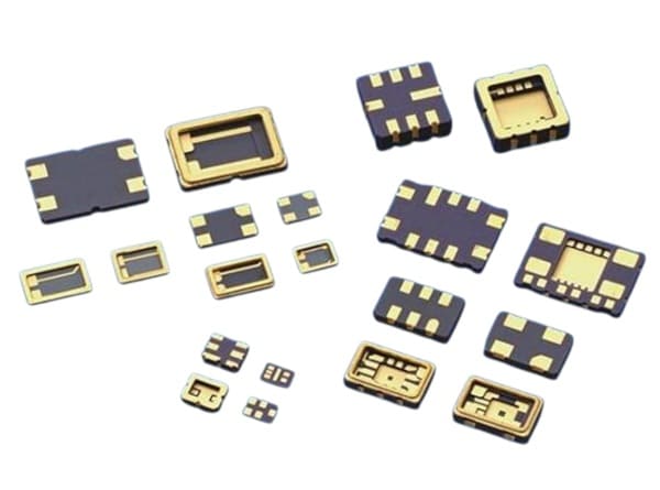
As electronic devices continue to shrink in size, traditional components and circuit designs can no longer meet space constraints. LTCC technology offers a solution by integrating multiple components into a single platform. By combining ceramic substrates with conductive materials (such as silver or copper), LTCC allows various functional elements like resistors, capacitors, and sensors to be embedded in a single ceramic substrate, significantly reducing the device’s volume. This is crucial for products with strict size requirements, such as smartphones, wearable devices, and medical equipment.
What Are the Materials Used in LTCC?
LTCC technology relies on carefully engineered materials to achieve its unique combination of high-frequency performance, thermal stability, and multilayer integration. The key material components include:
1. Ceramic Substrate Materials
The foundation of LTCC consists of glass-ceramic composites, chosen for their:
- Low sintering temperature (850–900°C)
- Controlled dielectric constant (Dk)
- Thermal expansion matching with semiconductors
Common LTCC Ceramic Systems:
| Material Composition | Key Properties | Typical Applications |
| Al₂O₃ + Glass (e.g., borosilicate) | Dk ~5–9, tanδ <0.005 | RF filters, antennas |
| Crystallizable Glass (e.g., MgO-Al₂O₃-SiO₂) | Dk ~4–7, high strength | Automotive sensors |
| Lead-free Glass Composites | RoHS compliant, Dk ~6–8 | Consumer electronics |
2. Conductor Materials
LTCC’s low firing temperature enables the use of high-conductivity metals (unlike HTCC, which requires refractory metals):
- Silver (Ag) – Most common (low cost, high conductivity)
- Gold (Au) – For high-reliability RF applications
- Copper (Cu) – Emerging option (oxidation-sensitive)
Key Requirements:
✔ Must sinter simultaneously with ceramics
✔ Minimal interfacial reactions (e.g., Ag diffusion into glass)
Looking for top-quality ceramic products? Explore the Advanced Ceramics Hub’s selection.
What Are the Manufacturing Processes of LTCC?
LTCC fabrication involves multiple precise steps to create multilayer ceramic substrates with embedded passives and interconnects. The key processes are:
1. Green Tape Preparation
Ceramic Slurry Formulation:
- Mix glass-ceramic powder (e.g., Al₂O₃ + borosilicate glass) with organic binders/solvents.
Tape Casting:
- Spread slurry into thin sheets (50–200 μm) using doctor-blade or roll-to-roll methods.
- Dry to form flexible “green tapes.”
2. Via Formation & Filling
- Laser Drilling/Mechanical Punching: Create micro-vias (50–150 μm diameter) for vertical interconnects.
- Via Filling: Screen-print conductive paste (Ag/Au) into vias using stencils or inkjet printing.
3. Screen Printing
- Conductor Printing: Deposit electrode patterns (traces, pads) with Ag/Au pastes (line width ≥50 μm).
- Passive Integration: Print resistor (RuO₂) or dielectric (BaTiO₃) pastes for embedded components.
4. Layer Stacking & Lamination
- Alignment: Stack printed layers with optical alignment (±25 μm tolerance).
- Isostatic Lamination: Apply heat (60–80°C) and pressure (10–30 MPa) to bond layers.
5. Co-firing (Sintering)
Debinding:
- Heat at 300–500°C to burn out organic binders.
Sintering:
- Fire at 850–900°C (peak) in air/N₂ to densify ceramics/metals simultaneously.
- Shrinkage: 12–15% (compensated in design).
6. Post-Processing
- Laser Trimming: Adjust resistor values by laser ablation.
- Surface Finishing: Plate Ni/Au for wire bonding or solderability.
- Component Assembly: Attach ICs/SMDs via soldering or conductive adhesives.
Explore our optimized ceramic products.
What Are the Advantages of LTCC Technology?
LTCC technology offers a unique combination of performance, integration, and reliability, making it indispensable for advanced electronics. Below are its key advantages:
1. Superior High-Frequency Performance
✔ Ultra-Low Signal Loss
- Dielectric loss (tan δ) as low as 0.002–0.005, ideal for RF/microwave (5G, radar, satellite) applications.
- Stable dielectric constant (Dk 4–9) across GHz frequencies.
✔ Controlled Impedance
- Precise conductor patterning enables matched impedance traces, reducing signal reflections.
2. 3D Multilayer Integration
✔ Embedded Passive Components: Resistors, capacitors, and inductors can be integrated inside the substrate, saving PCB space.
✔ High-Density Interconnects: Supports 50+ layers with microvias (50–150 μm diameter) for compact module designs.
3. Excellent Thermal & Mechanical Stability
✔ Matched CTE: Thermal expansion coefficient (6–9 ppm/°C) aligns with Si/GaAs chips, reducing stress in packaging.
✔ High-Temperature Resistance: Operates reliably from –55°C to +150°C (suitable for automotive/aerospace).
4. Hermetic & Reliable Packaging
✔ Moisture/Chemical Resistance: Naturally airtight structure prevents oxidation and corrosion (critical for medical implants).
✔ Vibration & Shock Resistant: Robust ceramic structure withstands harsh environments (e.g., engine sensors).
5. Cost-Effective for Mid-Volume Production
✔ Lower Processing Temperature: Sinters at 850–900°C (vs. HTCC’s 1600°C), reducing energy costs.
✔ Material Savings: Combines PCB + IC packaging functions, eliminating separate RF components.
6. Design Flexibility
✔ Customizable Material Properties: Adjustable Dk, thermal conductivity, and mechanical strength.
✔ Hybrid Integration: Compatible with silicon, PCB, and thin-film technologies for heterogeneous systems.
Discover our high-quality ceramic products.
What Are the Applications of LTCC Technology?
LTCC technology is widely adopted across industries due to its high-frequency performance, miniaturization capabilities, and rugged reliability. Below are its key applications categorized by sector:
1. Wireless Communications & 5G/6G
a. RF Front-End Modules
- Smartphones: Antenna switches, duplexers, and power amplifiers (e.g., Murata’s LTCC-based RF modules for iPhones).
- 5G/6G Base Stations: Beamforming antennas, mmWave filters (24–100 GHz), and low-noise amplifiers (LNAs).
b. Satellite & Radar Systems
- Phased-array antennas for low-Earth orbit (LEO) satellites.
- Automotive radar: 77 GHz/79 GHz antenna substrates (e.g., Bosch radar sensors).
2. Automotive Electronics
a. Engine & Powertrain Control
- High-temperature sensors (e.g., knock sensors, exhaust gas pressure monitors).
b. Electric Vehicles (EVs)
- Battery management systems (BMS): Isolated current sensors with embedded passives.
- Onboard chargers (OBC): Compact DC-DC converters.
3. Medical & Healthcare Devices
a. Implantable Electronics
- Pacemakers & neurostimulators: Hermetic packaging prevents body fluid ingress.
- Continuous glucose monitors (CGMs): Miniaturized wireless sensor modules.
b. Diagnostic Equipment
- MRI-compatible RF coils, ultrasound transducers.
4. Aerospace & Defense
a. Avionics: Flight control sensors (vibration-resistant, EMI-shielded).
b. Military Communications: Secure RF transceivers, jam-resistant radar systems.
Request a custom quote for high-quality ceramic products.
The Comparison of LTCC With Other Alternative Technologies
| Parameter | LTCC | HTCC | Organic PCBs | Thin-Film | DBC |
| Firing Temp. | 850-900°C | 1500-1600°C | N/A (Laminated) | <400°C (Deposited) | 800-1000°C (Bonding) |
| Conductor Materials | Ag, Au, Cu | W, Mo | Cu | Au, Cu, Ni | Cu |
| Thermal Conductivity | 2-5 W/mK | 15-25 W/mK | 0.2-0.5 W/mK | 20-30 W/mK | 24-200 W/mK |
| Max Freq. Range | DC-100+ GHz | DC-40 GHz | DC-10 GHz | DC-THz | DC-MHz |
| Dielectric Loss (tanδ) | 0.002-0.005 | 0.001-0.003 | 0.02-0.05 | 0.0001-0.001 | 0.0005-0.002 |
| Feature Resolution | 50-100 μm | 30-50 μm | 10-20 μm | 1-10 μm | 100-500 μm |
| Layer Count | Up to 50+ | <30 | <20 | <10 | 1-2 |
| CTE (ppm/°C) | 6-9 (matches Si/GaAs) | 6-8 | 12-18 | 4-7 | 4-7 |
| Hermeticity | Naturally hermetic | Hermetic | Non-hermetic | Semi-hermetic | Hermetic |
| Power Handling | Medium-High | High | Low-Medium | Low | Very High |
| Cost | Moderate | High | Low | Very High | High |
| Key Advantages | RF performance, 3D integration | Extreme temp. stability | Low cost, mass production | Ultra-miniaturization | Extreme thermal management |
| Main Applications | 5G RF, automotive sensors | Aerospace, power electronics | Consumer electronics | MEMS, photonics | Power modules (EV/IGBT) |
Recent Advancements in LTCC Technology
In recent years, significant advancements have been made in LTCC technology. These include innovations in materials, design structures, and the integration of LTCC with other technologies.
Innovations in Materials:
Researchers have developed new composite materials that offer improved conductivity, thermal performance, and flexibility. These innovations have enabled LTCC technology to meet the demands of emerging applications, such as 5G communication and electric vehicles.
Development of Multi-Layer LTCC Structures:
Multi-layer LTCC systems allow for increased component density and more complex circuit designs. This advancement has opened doors for applications in high-performance electronics, where space and weight are crucial.
Integration with Microelectronics and MEMS:
LTCC is increasingly being integrated with microelectromechanical systems (MEMS) and microelectronics. This integration enhances the functionality of LTCC-based devices, making them more versatile and capable of serving a wide range of applications in sensors, actuators, and communication devices.
Advances in 3D LTCC Designs:
The development of 3D LTCC designs allows for even more compact and efficient systems. This innovation is particularly useful in applications where size and performance are critical, such as in automotive and medical electronics.
Miniaturization and Increased Functionality:
Miniaturization in electronics has advanced LTCC technology, enabling smaller, more powerful devices. It integrates multiple functions into a compact package, essential for space-constrained applications like mobile devices and IoT. Multi-functional integration of components like capacitors, inductors, and antennas within the ceramic substrate improves performance, reduces component count, and lowers costs.
At Advanced Ceramics Hub, we supply optimized-grade ceramic products that comply with ASTM and ISO standards, ensuring outstanding quality and reliability.
FAQ
| Question | Answer |
| What is LTCC technology? | LTCC (Low Temperature Cofired Ceramic) technology is a method of creating electronic circuits by embedding components in ceramic substrates. |
| What are the applications of LTCC technology? | LTCC is widely used in telecommunications, automotive, medical devices, sensors, and IoT due to its compactness, reliability, and versatility. |
| How does LTCC enable miniaturization in electronics? | LTCC allows the integration of multiple components into a compact package, reducing size while increasing functionality. |
| What are the benefits of multi-layer LTCC systems? | Multi-layer LTCC systems increase component density, enabling complex circuit designs and improving overall performance. |
| How does LTCC technology improve device reliability? | LTCC enhances device reliability by embedding components directly into the ceramic substrate, reducing the risk of failure. |
| What is the future potential of LTCC technology? | LTCC’s future lies in its ability to support 5G, electric vehicles, and advanced medical applications, offering compact and high-performance solutions. |
LTCC technology has established itself as a vital enabler of modern electronics, offering unparalleled reliability, thermal stability, and performance in high-frequency applications. From RF circuits to medical devices, LTCC’s versatility has made it indispensable across industries. While challenges like cost and scalability remain, ongoing advancements in materials, miniaturization, and flexible substrates are expanding its potential.
For top-quality ceramic products, Advanced Ceramics Hub provides tailored solutions and precision machining techniques for various applications.
Looking for premium ceramic products? Contact us today!