6 Key Interface Challenges in Thermal Conductive Materials and How to Solve Them
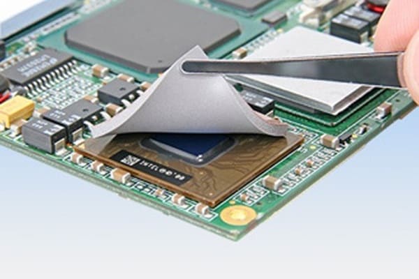
Thermal conductive materials play a pivotal role in modern technology, serving as the backbone for efficient heat dissipation in a wide array of applications, from consumer electronics to aerospace systems. These materials, often referred to as Thermal Interface Materials (TIMs), bridge the gap between heat-generating components and heat sinks, ensuring that excess heat is transferred away to prevent overheating and maintain optimal performance.
However, in practical applications, various interface issues are often encountered. These problems may seem trivial, but they can significantly impact the performance of thermal interface materials, ultimately affecting the heat dissipation efficiency and stability of electronic devices. Let’s take a closer look at some common interface problems in thermal interface materials.
1. Contact Thermal Resistance: The “Roadblock” to Heat Transfer
What is Contact Thermal Resistance?
Contact thermal resistance (also known as interfacial thermal resistance) occurs when two surfaces meet but fail to achieve perfect thermal conduction due to microscopic gaps, surface roughness, or material mismatches. These imperfections trap air or create voids, acting as insulating barriers that hinder efficient heat transfer.
Key Factors Influencing Contact Thermal Resistance
Surface Roughness
- Rougher surfaces reduce effective contact area, creating air gaps that act as thermal barriers.
- Example: Polished metals exhibit ~50% lower contact resistance than rough surfaces.
Contact Pressure
- Higher pressure deforms surface asperities, increasing real contact area.
- Data: Increasing pressure from 0.1 MPa to 1 MPa can reduce steel-steel contact resistance by 40%.
Material Thermal Conductivity
- High-κ materials (e.g., copper) inherently have lower interfacial resistance vs. insulators (e.g., ceramics).
- Note: Bulk κ ≠ interfacial κ—surface treatments remain critical.
Why It’s a Critical Challenge
- Heat Flow Disruption: Even high-conductivity materials (like graphene or metals) suffer when interfacial gaps impede heat dissipation.
- Performance Loss: In electronics, excessive contact resistance can lead to overheating, reducing efficiency and lifespan.
- Real-World Impact: From CPU heat sinks to battery thermal management, poor interfacial contact can derail system reliability.
2. Wettability Issues: The “Lack of Affinity” Between Materials
The Problem: Poor Thermal Contact Due to Weak Adhesion
Wettability refers to a material’s ability to maintain intimate contact with another surface, typically influenced by surface energy and adhesion forces. Poor wettability leads to:
- Air gaps & voids at interfaces, increasing thermal resistance.
- Incomplete spreading of thermal interface materials (TIMs) reduces the effective heat transfer area.
- Delamination risks under thermal cycling due to weak bonding.
Key Factors Affecting Wettability
Surface Energy Mismatch
- High-energy surfaces (e.g., metals) promote better wetting than low-energy ones (e.g., polymers).
- Example: Copper (high surface energy) pairs well with solder, while untreated plastics repel TIMs.
Contamination & Oxidation
- Oils, oxides, or residues create hydrophobic barriers.
- Solution: Plasma cleaning or chemical flux removes contaminants before bonding.
Viscosity of Thermal Interface Materials (TIMs)
- Low-viscosity TIMs (e.g., liquid metal) spread easily but may pump out.
- High-viscosity TIMs (e.g., greases) resist flow, risking uneven coverage.
Surface Texture & Porosity
- Rough or porous surfaces can either enhance capillary action (improving wetting) or trap air (worsening it).
3. Pumping Phenomenon: The Material’s “Runaway”
The pumping phenomenon occurs when thermal interface materials (TIMs) gradually migrate or are squeezed out from between mating surfaces under thermal cycling or mechanical stress. This “material runaway” leads to:
- Progressive degradation of thermal contact over time
- Formation of dry spots where heat transfer becomes inefficient
- Increased thermal resistance as the TIM layer becomes thinner or uneven
- Potential contamination of surrounding components
Key Causes of Pumping Effect
Thermal Cycling Stress
- Repeated expansion/contraction creates a “pumping” action that pushes TIM out
- Common in power electronics with frequent load changes
Mechanical Pressure
- Excessive clamping force can squeeze out softer TIMs
- Particularly problematic with low-viscosity greases and phase-change materials
Material Properties
- Low-viscosity TIMs are more prone to migration
- Thermally unstable formulations may break down under stress
Surface Characteristics
- Smooth surfaces offer less “grip” for TIM retention
- Certain surface finishes may accelerate material creep
4. Drying and Phase Separation: The Material’s “Degradation Crisis”
Drying and phase separation occur when thermal interface materials (TIMs) lose their structural integrity over time, leading to:
- Formation of dry, brittle regions that increase thermal resistance
- Separation of filler particles from the matrix, destroying thermal pathways
- Cracking and shrinkage, creating air gaps at critical interfaces
- Catastrophic failure in high-reliability applications
Key Causes of TIM Degradation
1. Polymer Base Deterioration
- Oxidation: Exposure to air/heat breaks down organic binders (especially silicones)
- Volatile Loss: Plasticizers or solvents evaporate over time
- Thermal Cracking: Repeated thermal cycling fractures polymer chains
2. Filler Settling & Agglomeration
- Density Mismatch: Heavy ceramic/metallic particles sink in liquid matrices
- Poor Dispersion: Inadequate mixing leads to particle clustering
- Surface Chemistry: Unmodified fillers repel the matrix material
3. Environmental Attacks
- Humidity Absorption: Hydrolysis of ester-based TIMs
- Chemical Exposure: Ozone, acids, or solvents degrade materials
- UV Radiation: Sunlight accelerates polymer breakdown
5. Interfacial Delamination and Debonding: The “Breakdown” of an Intimate Bond
Interfacial delamination occurs when bonded surfaces separate, creating insulating air gaps that:
- Increase thermal resistance exponentially (up to 1000× in severe cases)
- Causes localized overheating and hot spots
- Lead to mechanical failure through crack propagation
- Result ina complete system breakdown in power electronics and high-density packaging
Mechanisms of Bond Failure
1. Stress-Induced Delamination
- CTE Mismatch: Differing thermal expansion creates shear stress
- Mechanical Shock: Vibration or impact fractures weak interfaces
- Curing Shrinkage: Polymer TIMs contracting during solidification
2. Adhesion Failure Modes
- Cohesive Failure: TIM tears internally (material weakness)
- Adhesive Failure: Bond separates from substrate (interface weakness)
- Mixed-Mode Failure: A Combination of both
3. Environmental Attackers
- Moisture Ingression: Hydrolysis of adhesive bonds
- Thermal Aging: Polymer degradation at high temperatures
- Chemical Exposure: Solvents weaken interfacial bonds
6. Void and Bubbles: Hidden “Thermal Insulation Traps”
Microscopic voids and bubbles in thermal interface materials (TIMs) act as:
- Thermal barriers (air κ≈0.026 W/mK vs. TIM κ≈1-10 W/mK)
- Stress concentrators that initiate cracks and delamination
- Performance killers that can increase thermal resistance by 300-500%
Key Causes
| Category | Specific Causes |
| Process Issues | – Excessive dispensing speed introduces air – Uneven squeegee pressure during screen printing – Incomplete mold filling |
| Material Issues | – Poor outgassing properties during curing – High viscosity limits flow and gap-filling capability |
| Surface Issues | – Complex microstructures trap air – Excessive surface roughness creates local voids |
The interface issues faced by thermal interface materials in practical applications are not to be ignored. These issues interact with each other and collectively limit the performance of thermal interface materials, thereby impacting the heat dissipation effectiveness and reliability of electronic devices. In the following, we’ll take a look at the effective strategies and technologies they have adopted.
How to Identify Interface Issues?
Faced with various interface issues of thermal interface materials in practical applications, how can we accurately detect and analyze them? This requires the use of a series of advanced characterization and evaluation techniques, which help us gain a deep understanding of the microstructure and performance of thermal interface materials, and thus pinpoint the root causes of the problems.
Thermal Performance Parameter Testing
Thermal impedance, thermal resistance, and thermal conductivity are key thermal performance parameters for evaluating thermal interface materials. They serve as the “health indicators” of these materials, and by measuring these parameters, we can uncover potential issues within the thermal interface material through the numbers.
Thermal resistance:
Thermal resistance measures how much a material resists heat transfer, defined as the ratio of temperature difference to heat flow, with units of K/W. Higher thermal resistance means more difficulty in heat transfer. In thermal interface materials, contact thermal resistance significantly affects heat dissipation efficiency. Measuring it helps identify issues like poor contact, voids, or bubbles. High thermal resistance suggests large contact thermal resistance, requiring further inspection of the interface’s microstructure.
Thermal conductivity:
Thermal conductivity measures a material’s ability to conduct heat, with units of W/(m·K). Higher conductivity means better heat transfer. For thermal interface materials, high conductivity is crucial for efficient heat dissipation. Different materials, like pastes, pads, and gels, have varying conductivities. Measuring conductivity helps assess whether the material meets thermal performance requirements and identifies issues like uneven filler dispersion or material aging if conductivity is lower than expected.
Key Testing Methods
Steady-State Methods:
✅Guarded Hot Plate Method
- High accuracy
- Suitable for various materials
- Complex equipment, longer measurement time
✅Heat Flow Meter Method
- Easy to operate
- Faster measurement
- Lower accuracy compared to the guarded hot plate method
Transient Methods:
✅Hot Wire Method
- Suitable for materials with low thermal conductivity
- Fast measurement
- Limited accuracy
✅Laser Flash Method
- High precision
- Measures thermal diffusivity and conductivity
- Fast and non-contact operation
Microscopic Structure Observation
To gain a deeper understanding of the interface issues in thermal interface materials, it is not enough to rely solely on thermal performance parameter testing. We also need to delve into the microscopic world and observe the microstructure of the thermal interface materials. Techniques such as Scanning Electron Microscopy (SEM), C-SAM (C-mode Scanning Acoustic Microscopy), and X-ray imaging have opened the door to the microscopic world for us.
✅Infrared Thermography:
- Reveals localized hot spots
- Shows thermal resistance distribution
- Example: 20°C variation indicates poor contact
✅Ultrasound Inspection:
- Detects delamination/voids
- Measures bond integrity
- Sensitivity: Can find 50μm defects
✅X-Ray/CT Scanning:
- 3D void mapping
- Non-destructive internal inspection
- Resolution down to 1μm
Interface Performance Testing
In addition to thermal performance parameter testing and microscopic structure observation, interface performance testing is also a crucial method for evaluating the performance of thermal interface materials. Techniques such as adhesion testing, contact angle measurement, rheological property testing, and coefficient of thermal expansion measurement can help us gain a comprehensive understanding of the interactions between the thermal interface material and the contact surface, as well as the inherent properties of the material itself.
Adhesion Strength
Adhesion strength refers to the bonding force between thermal interface materials and the contact surface. It directly impacts the stability and reliability of thermal interface materials. The purpose of adhesion testing is to measure the magnitude of this bonding force. Common testing methods include:
- Tensile Test: The thermal interface material is bonded to the contact surface, and a tensile force is applied. The force required to separate the two materials is measured to determine the adhesion strength.
- Peel Test: The thermal interface material is gradually peeled from the contact surface, and the force-displacement relationship during the peeling process is measured to calculate the adhesion strength.
- Shear Test: Shear force is applied parallel to the interface to measure the material’s resistance to shear deformation.
Adhesion testing helps assess the bonding performance of thermal interface materials with different substrates, determining whether delamination or debonding may occur. If the adhesion strength is insufficient, measures such as surface treatment or adding adhesion promoters may be necessary to enhance the bond.
Contact Angle
The contact angle is an important parameter for assessing the wetting behavior of liquids on solid surfaces, reflecting the interaction between the liquid and the solid surface. In thermal interface materials, the contact angle directly affects the material’s wettability. When the material is in a liquid or semi-liquid state, its wetting behavior on the contact surface significantly influences the filling effect and thermal resistance.
- Measurement Principle: Based on the shape of a droplet on a solid surface, the contact angle is determined by measuring the angle between the droplet and the surface.
- Small Contact Angle: Indicates good wetting ability, allowing the liquid to spread well on the surface, improving wettability.
- Large Contact Angle: Suggests poor wetting, making it difficult for the liquid to spread and potentially creating air gaps, which increases thermal resistance.
By measuring the contact angle, we can assess the wettability of thermal interface materials and improve the filling effect.
Rheological Properties
Rheological properties refer to the flow and deformation characteristics of materials under stress, which directly impact the processing performance of thermal interface materials during preparation and use. Rheological testing helps us understand parameters such as viscosity, elastic modulus, and thixotropy.
- Viscosity: A measure of the resistance to fluid flow. If the viscosity is too high, the material will be difficult to apply or fill during the process, affecting workability. If the viscosity is too low, the material may be extruded during use, increasing thermal resistance.
- Elastic Modulus: Reflects the material’s ability to resist elastic deformation. For applications that involve mechanical vibrations or thermal cycles, an appropriate elastic modulus ensures stable performance under stress.
- Thixotropy: The ability of a material to undergo viscosity changes over time when subjected to shear forces. Materials with good thixotropic properties become less viscous under external force, making them easier to apply and fill, and return to their original viscosity when the force is removed, preventing displacement during use.
Rheological performance testing helps optimize the formulation of thermal interface materials to improve both processing and usage performance.
Coefficient of Thermal Expansion (CTE)
The coefficient of thermal expansion (CTE) is the ratio of length or volume change of a material due to temperature variation. It is an important parameter for assessing the thermal compatibility of thermal interface materials with the contact surface. As thermal interface materials and the contact surfaces are often composed of different materials, their CTEs may differ.
- Thermal Stress: When temperature changes, the difference in CTEs generates thermal stress at the interface. If thermal stress is too high, it can lead to delamination or debonding.
- Measurement Methods: Techniques such as thermomechanical analysis (TMA) and laser interferometry are commonly used to measure the CTE.
By measuring the CTE, we can understand the thermal expansion compatibility between thermal interface materials and contact surfaces, which aids in selecting the appropriate material combination and optimizing interface design. In practical applications, it is desirable for the CTE of the thermal interface material to closely match that of the contact surface to minimize thermal stress.
Solutions to Interface Challenges
Researchers and engineers have actively explored and proposed a series of effective strategies to address the various interface issues encountered in the practical application of thermal interface materials. These strategies focus on multiple aspects, including material optimization, interface treatment, process improvements, and structural innovations, with the goal of reducing thermal resistance at the interface, enhancing the performance of thermal interface materials, and ensuring efficient heat dissipation and stable operation of electronic devices.
1. Material Optimization Strategies
Material optimization is one of the key strategies for addressing interface issues in thermal interface materials. It focuses on the selection and design of materials, aiming to enhance material performance from the source and reduce the occurrence of interface problems.
Matrix Material Selection
| Matrix Type | Key Properties | Typical Applications | Thermal Conductivity Range |
| Silicone Grease | Low viscosity, good wettability | CPU/GPU cooling | 0.5-5 W/m·K |
| Epoxy Resin | High strength, chemical resistance | Power electronics | 1-10 W/m·K |
| Polyimide | High temp stability (>300°C) | Aerospace, automotive | 0.5-15 W/m·K |
| Liquid Metal | Ultra-high conductivity | High-power devices | 15-80 W/m·K |
Filler Material Engineering
A. Filler Types by Material Class
| Category | Examples | κ (W/m·K) | Key Advantages |
| Metals | Ag, Cu | 429, 401 | Highest conductivity |
| Ceramics | AlN, BN, Al₂O₃ | 200-320 | Electrically insulating |
| Carbon Allotropes | Graphene, CNT, Diamond | 5300, 3000, 2000 | Anisotropic conduction |
B. Filler Morphology Optimization
| Morphology | Benefits | Challenges | Best For |
| Spherical | Good dispersion, flowability | Limited percolation | Low-pressure applications |
| Flake | High in-plane κ, low loading threshold | Orientation sensitivity | TIM pads, sheets |
| Fibrous | Continuous thermal pathways | Viscosity increase | Polymer composites |
Advanced Filler Formulation Strategies
A. Size Distribution Design
| Particle Size | Role | Optimal Loading |
| Nano-scale (<100nm) | Fills microscopic gaps, reduces contact resistance | 5-15 vol% |
| Micro-scale (1-50μm) | Primary heat conduction | 40-70 vol% |
| Hybrid Systems | Nano fills micro voids | 50-80 vol% total |
B. Surface Modification Techniques
- Silanization: Improves filler-matrix bonding
- Polymer grafting: Prevents agglomeration
- Metallization: Enhances particle-particle contact
- Interface Treatment: Achieving Perfect Bonding
2. Interface Treatment: Achieving Perfect Bonding
Interface treatment technology is one of the key methods for addressing interface issues in thermal interface materials. By applying various treatments to the contact surfaces, it aims to improve the wettability and adhesion at the interface, reduce thermal resistance, and ensure a seamless bond between the thermal interface material and the contact surface.
A. Surface Cleaning Methods
| Technique | Mechanism | Advantages | Limitations | Typical Applications |
| Plasma Cleaning | Reactive species oxidation | Non-contact, <5nm cleanliness | Requires vacuum | High-performance electronics |
| Solvent Wiping (IPA/acetone) | Dissolution of contaminants | Fast, low-cost | Residual streaks | General-purpose cleaning |
| Laser Ablation | Instant vaporization | No chemicals, <1μm precision | High equipment cost | Delicate substrates |
B. Surface Activation Approaches
| Method | Surface Modification | Effect on Surface Energy | Performance Improvement |
| Plasma Treatment | Introduces -OH/-COOH groups | 50→70+ dynes/cm | 40% better TIM wettability |
| Chemical Etching | Creates micro-roughness | Increases effective area | 30% lower contact resistance |
| Laser Texturing | Forms hierarchical structures | Enhances mechanical interlock | 50% stronger adhesion |
C. Surface Coating Strategies
| Coating Type | Deposition Method | Key Benefits | Thickness Range |
| Metallic Layers (Cu/Ni) | Electroplating/sputtering | Low Rth, oxidation barrier | 1-20μm |
| Organosilane Primers | Spin-coating/spraying | Improved TIM adhesion | 0.1-1μm |
| Carbon Nano-interlayers | CVD/transfer | Graphene-enhanced conduction | 2-50nm |
D. Surface Structuring Techniques
| Structure | Fabrication Process | Thermal Benefit |
| Micro-pillars | Photolithography + DRIE | 35% lower Rth |
| Hierarchical grooves | Laser ablation | 25% better heat spreading |
| Inverse opals | Template deposition | Anisotropic cooling |
Implementation Guidelines by Material Type
| Substrate | Recommended Process Flow |
| Aluminum Heat Sinks | 1. Alkaline degrease → 2. Anodization → 3. Silane primer |
| Copper Spreaders | 1. Acid pickling → 2. Micro-etching → 3. Antioxidant coating |
| Ceramic Packages | 1. Plasma clean → 2. Ti/Ni metallization → 3. Laser patterning |
3. Process Improvement: The Devil is in the Details
Process improvement is a crucial step in enhancing the performance of thermal interface materials. It focuses on multiple aspects, including coating, curing assembly, bubble removal, and pressure control. By optimizing every detail, it ensures that thermal interface materials can deliver optimal performance in electronic devices.
A. Deposition Techniques Comparison
| Method | Resolution | Throughput | Best For | Key Parameters |
| Automated Dispensing | ±50μm | Medium | Complex patterns | Needle size, flow rate, path planning |
| Screen Printing | ±100μm | High | Large-area coating | Mesh count, squeegee pressure, snap-off |
| Inkjet Printing | ±20μm | Low | Ultra-fine features | Drop volume, firing frequency |
| Electrospray | ±10μm | Low | Nanoscale films | Voltage, flow rate, collector distance |
B. Curing Process Optimization
Critical Control Factors
Pressure Requirements:
- Bondline thickness control: 25-100μm typically
- Optimal range: 10-50 psi (varies by TIM type)
Temporal Factors:
- Minimum 90% cure before thermal cycling
- Post-cure stabilization (4- 8 hours recommended)
- Vacuum-Assisted Processes
C. Vacuum-Assisted Processes
| Technology | Vacuum Level | Bubble Reduction | Equipment |
| Batch Vacuum Lamination | 10-2 Torr | >90% | Chamber systems |
| In-line Degassing | 10-1 Torr | 70-80% | Rotary vane pumps |
| Micro-Vacuum Dispensing | 100 Torr | 50-60% | Integrated nozzles |
D. Pressure Management Solutions
| Approach | Mechanism | Accuracy | Application |
| Spring Loaded | Constant force | ±15% | Consumer electronics |
| Pneumatic | Air pressure regulated | ±5% | Automotive |
| Shape Memory Alloys | Temperature-responsive | ±2% | Aerospace |
4. Structural Innovation: Paving the Way for New Solutions
With the continuous advancement of technology, structural innovation in thermal interface materials has emerged as a new direction for addressing interface issues. Researchers are exploring new structures and material forms, opening up fresh avenues for enhancing the performance of thermal interface materials.
A. Phase Change Materials (PCMs)
- Mechanism: Solid-liquid transition fills microgaps when heated
- Pros: Low thermal resistance (~0.05 cm²·K/W), latent heat absorption
- Cons: Pump-out risk during thermal cycling
Innovations:
- Microencapsulation prevents leakage
- Polymer-thickened formulations enhance stability
- Common base: Paraffin wax with metal/ceramic fillers
B. Thermal Gels & Elastomers
Gels:
- Semi-solid, >80% conformality to rough surfaces
- Ideal for smartphones (0.5-3 W/m·K range)
- Self-adhesive versions simplify assembly
Elastomers:
- Shore hardness 20-50 for vibration resistance
- Automotive-grade variants withstand 50G shocks
- Often silicone-based with AlN/BN fillers
C. Thermal Pads
- Pre-formed sheets (0.1-5mm thickness)
- Surface engineering: Micro-domes enhance contact by 30% at low pressure, while anisotropic versions direct heat vertically.
- Trade-off: Typically lower κ (1-6 W/m·K) vs. greases
D. Metal-Based TIMs
Liquid Metals (e.g., Ga-In-Sn):
- Ultra-high κ (~30 W/m·K) but corrosive
- Requires nickel/gold plating on surfaces
Indium Foils:
- Soft compensates for CTE mismatch
- Used in aerospace (reliability >100,000 cycles)
Solders:
- Permanent bonds for high-power modules
- Processing challenges (reflow temps >200°C)
E. 3D Structured TIMs
Vertical CNT Arrays:
- κ >1,500 W/m·K along tubes
- Grown directly on substrates to eliminate interfaces
Graphene Foams:
- 3D porous networks (κ ~500 W/m·K)
- Compressible for varying gap tolerances
Hybrid Architectures:
- CNT-graphene sandwiches for isotropic cooling
- Metal-coated polymer scaffolds
In conclusion, addressing the six key interface challenges in thermal conductive materials is essential to improving the performance and longevity of thermal management systems. By using advanced materials, optimized bonding techniques, and innovative manufacturing methods, these challenges can be overcome. As the demand for more efficient and durable thermal solutions grows across industries, further research and development in this field will continue to drive improvements in both material performance and design.
For top-quality ceramic products, Advanced Ceramics Hub provides tailored solutions and precision machining techniques for various applications.
Looking for premium thermal interface material products? Contact us today!