How Does Wurtzite Boron Nitride Improve the Performance of Electronic Devices?
Wurtzite boron nitride (w-BN) is an advanced material gaining attention in the electronics industry due to its remarkable properties as a wide-bandgap semiconductor. As modern electronic devices demand higher efficiency, faster performance, and greater durability, materials like w-BN are pivotal in pushing the boundaries of technology. Unlike traditional materials such as silicon, w-BN offers unique physical and electronic characteristics that make it ideal for next-generation applications, from high-power electronics to optoelectronic systems. Its ability to operate under extreme conditions, such as high voltages and temperatures, positions it as a game-changer in fields like electric vehicles, telecommunications, and renewable energy.
The significance of advanced materials in electronics cannot be overstated. As devices become smaller, more powerful, and more energy-efficient, the limitations of conventional semiconductors become apparent. Silicon, for instance, struggles to maintain performance in high-temperature or high-voltage environments. w-BN addresses these challenges by combining a wide bandgap, high thermal conductivity, and exceptional stability. This article explores how w-BN enhances the performance of electronic devices through its unique properties, offering insights into its applications, benefits, and future potential.
At Advanced Ceramics Hub, we specialize in high-quality boron nitride ceramic products with various forms and specifications, ensuring optimal performance for industrial and scientific applications.
Properties of Wurtzite Boron Nitride
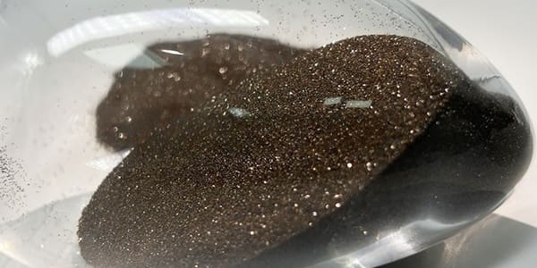
Wurtzite boron nitride is a polymorph of boron nitride, characterized by a hexagonal crystal structure similar to that of wurtzite zinc oxide. Unlike cubic boron nitride (c-BN), which is known for its diamond-like hardness, w-BN is distinguished by its semiconductor properties. Its crystal lattice consists of alternating boron and nitrogen atoms, forming a robust structure that contributes to its unique electrical and thermal characteristics. This structure enables w-BN to outperform many traditional semiconductors in extreme conditions, making it a promising material for advanced electronics.
1. Structural Properties of Wurtzite Boron Nitride
Wurtzite Boron Nitride (w-BN) is a crystal structure of boron nitride, where the atoms are arranged in a hexagonal form, much like graphite. This structure gives it several unique characteristics, including high thermal conductivity, electrical insulating properties, and mechanical strength. While hexagonal Boron Nitride (h-BN) is commonly used, w-BN has superior properties due to its unique crystal arrangement.
Key Structural Benefits of Wurtzite Boron Nitride (w-BN):
- Superior Thermal Conductivity: Wurtzite BN exhibits high thermal conductivity due to its layered structure, making it ideal for heat dissipation in electronic devices.
- Electrical Insulation: Unlike materials like metals or graphite, w-BN acts as an electrical insulator, providing safety in high-voltage applications.
- Mechanical Strength: The crystal structure of w-BN gives it high strength and durability, helping electronic devices withstand physical stress.
2. Mechanical Properties of Wurtzite Boron Nitride (w-BN)
Wurtzite Boron Nitride’s high mechanical strength is another major advantage. The structure of w-BN enables it to resist deformation, fracturing, and abrasion under stress, making it an ideal material for harsh electronic environments.
Comparison with Other Superhard Materials:
| Property | w-BN | c-BN | Diamond | h-BN |
| Hardness (GPa) | ~50-60 | 45-50 | 70-100 | <5 |
| Fracture Toughness (MPa·√m) | 4.5-5.5 | 6-8 | 5-10 | 1-2 |
| Elastic Modulus (GPa) | 850-900 | 750-800 | 1050-1200 | 30-40 |
| Density (g/cm³) | 3.49 | 3.48 | 3.52 | 2.27 |
3. Thermal Properties of Wurtzite Boron Nitride (w-BN)
One of the most valuable features of w-BN is its thermal conductivity. Electronics generate heat during operation, and managing this heat is crucial for maintaining device performance and longevity. The high thermal conductivity of w-BN allows it to efficiently transfer heat away from heat-sensitive components, such as power transistors, LEDs, and semiconductors.
Key Thermal Characteristics:
| Property | w-BN Value | Comparison Benchmark |
| Thermal Conductivity (300K) | 200-250 W/m·K (∥c-axis) 120-150 W/m·K (⊥c-axis) | > Diamond (1000-2000 W/m·K) > c-BN (740 W/m·K) |
| Thermal Expansion Coefficient | 1.5×10⁻⁶ /K (∥c-axis) 2.8×10⁻⁶ /K (⊥c-axis) | < Alumina (8×10⁻⁶ /K) > Diamond (1×10⁻⁶ /K) |
| Specific Heat Capacity | 0.63 J/g·K @ 25°C | Similar to c-BN (0.64 J/g·K) |
| Phase Transition Temp. | 1700°C (w-BN → c-BN) | Higher than h-BN (stable to 1400°C) |
Thermal Stability Performance:
Oxidation Resistance:
✅ Stable in air up to 800°C (forms protective B₂O₃ layer)
✅ Outperforms diamond (oxidizes at 700°C)
Thermal Shock Resistance:
✅ Moderate (between c-BN and diamond)
✅ Survives 100+ cycles of 25°C⇄1200°C quenching
Advantages of w-BN in Thermal Management:
- Effective Heat Dissipation: w-BN ensures that excess heat is removed from critical components, reducing the risk of overheating and failure.
- High-Performance Devices: Applications in high-power electronics, LEDs, and semiconductors benefit from w-BN’s ability to manage heat effectively.
- Thermal Stability: The high temperature tolerance of w-BN enhances the longevity of devices, ensuring they remain functional in extreme environments.
Thermal Conductivity Comparison:
| Material | TC (W/m·K) | Temp. Stability |
| Diamond | 1000-2000 | <700°C (air) |
| w-BN | 200-250 | <800°C (air) |
| SiC | 490 | <1600°C |
| AlN | 320 | <1000°C |
4. Electronic Properties of Wurtzite Boron Nitride (w-BN)
In many high-voltage applications, electrical insulation is essential to prevent short circuits and protect sensitive components. w-BN serves as an excellent electrical insulator, providing safety and reliability in electronic devices that operate under high voltages.
| Property | w-BN | Comparison |
| Band Gap | 6.4 eV (direct) | > Diamond (5.5 eV) > GaN (3.4 eV) |
| Electron Mobility | ~300 cm²/V·s | < GaN (440 cm²/V·s) |
| Hole Mobility | ~150 cm²/V·s | Limited by self-trapping |
| Dielectric Constant | 4.5 (static) 3.8 (high freq.) | Similar to SiO₂ |
5. Chemical Stability and Corrosion Resistance of Wurtzite Boron Nitride (w-BN)
- BN exhibits remarkable chemical stability, even in reactive environments. This characteristic makes it highly resistant to corrosion, oxidation, and chemical degradation, which is crucial for devices exposed to harsh chemicals, high humidity, or extreme temperatures.
| Environment | w-BN Resistance | Notes |
| Air/Oxygen | Up to 1000°C | Forms B₂O₃ layer above 800°C |
| Acids | Excellent | Resists all except HF/HNO₃ mixes |
| Molten Metals | Excellent | Non-wetting to Al, Cu, Fe |
| Alkalis | Good | Attacks slowly above 500°C |
These properties collectively make w-BN a superior choice for applications requiring high efficiency, thermal management, and durability.
Looking for top-quality boron nitride products? Explore Advanced Ceramics Hub’s selection.
Applications of Wurtzite Boron Nitride (w-BN) in Electronic Devices
1. High-Power Electronics
w-BN’s wide bandgap and high breakdown field make it an excellent candidate for high-power electronics, such as power transistors and diodes used in energy conversion systems. These components are critical in applications like electric vehicles (EVs), where efficient power management directly impacts range and performance. For example, w-BN-based transistors can handle higher voltages with lower energy losses compared to silicon, leading to more efficient inverters for EV motors. Similarly, in renewable energy systems like solar inverters or wind turbines, w-BN enables compact, high-efficiency power conversion, reducing system size and cost.
| Device Type | Performance Benefit | Current Status |
| Ultra-HV Diodes | Blocking voltage >15 kV (vs. 3-5 kV for SiC) | Lab-scale demonstrated |
| RF Power Transistors | Reduced on-resistance at GHz frequencies | DARPA-funded development |
| Solid-State Circuit Breakers | Faster switching, zero arcing | Prototype testing (ABB) |
2. High-Frequency Devices
The high carrier mobility of w-BN makes it ideal for high-frequency applications, such as radio-frequency (RF) and microwave devices. These devices are essential for modern communication systems, including 5G and emerging 6G networks, as well as radar technologies used in aerospace and defense. w-BN’s ability to support fast electron movement ensures low signal loss and high switching speeds, enabling faster data transmission and improved signal integrity. For instance, w-BN-based RF amplifiers could enhance the performance of base stations in telecommunications.
Why w-BN Outperforms GaN/SiC?
| Property | w-BN | GaN | SiC |
| Bandgap (eV) | 6.4 (direct) | 3.4 | 3.3 |
| Breakdown Field (MV/cm) | 10 | 3.3 | 2.5 |
| Electron Mobility (cm²/V·s) | 300 (bulk) 2000 (2DEG) | 440 | 950 |
| Thermal Conductivity (W/m·K) | 200-250 | 130 | 490 |
3. Optoelectronics
With its wide bandgap, w-BN is well-suited for optoelectronic applications, particularly in ultraviolet (UV) light-emitting diodes (LEDs) and photodetectors. These devices are used in deep UV sterilization systems, optical communication, and scientific instrumentation. The ability of w-BN to emit and detect UV light efficiently stems from its bandgap, which corresponds to the UV wavelength range. This opens up possibilities for compact, energy-efficient UV devices that outperform those made from traditional materials like gallium nitride.
Why w-BN?
- 6.4 eV bandgap → Solar-blind detection (200-280 nm)
- High radiation hardness → Space/defense applications
Device Implementations:
✅DUV Photodetectors
- Detect flames/UV-C without solar interference
- EQE >60% @ 220 nm (AlGaN detectors: ~40%)
✅UV LEDs/Lasers
- Potential for 229 nm emission (unachievable with AlGaN)
Performance Comparison:
| Parameter | w-BN Device | AlGaN Device |
| Dark Current | 0.1 pA | 10 pA |
| Response Speed | 8 ns | 20 ns |
| Radiation Tolerance | 100 Mrad(Si) | 10 Mrad(Si) |
4. Quantum/Heterostructure Devices
Unique Properties Utilized:
- Atomically smooth surface (RMS roughness <0.2 nm)
- Near-perfect lattice match to graphene (1.7% mismatch)
Cutting-edge Applications:
A. Single-Photon Emitters
- Room-temperature operation (vs. cryogenic diamond NV centers)
- Telecom wavelength compatibility (via strain engineering)
- 2D Heterostructure Substrates
B. Heterostructure Substrates
Graphene/w-BN stacks enable:
- Electron mobility >200,000 cm²/V·s (10× freestanding graphene)
- Quantum Hall effect at 300K
C. Topological Insulator Interfaces
- w-BN/Bi₂Se₃ shows protected surface states up to 500K
5. Thermal Management Solutions
Thermal Conductivity Advantage:
- 200-250 W/m·K (isotropic average)
- CTE match to GaN/SiC (reduces thermal stress)
Implementations:
- 3D-IC Heat Spreaders: 30% lower hotspot temp vs. diamond films in TSV architectures
- Laser Diode Heat Sinks: Enables 50 W/mm output power for industrial lasers
Discover our high-quality boron nitride products.
Performance Improvements Enabled by Wurtzite Boron Nitride (w-BN)
Efficiency
w-BN significantly enhances the efficiency of electronic devices by reducing energy losses. Its high breakdown electric field allows devices to operate at higher voltages without failure, thereby minimizing power dissipation in components such as transistors and diodes. In high-frequency applications, w-BN’s high carrier mobility enables faster switching speeds, reducing energy losses during signal transitions. For example, in a power converter, w-BN-based components could achieve efficiencies exceeding 95%, compared to 85-90% for silicon-based systems.
Thermal Management
Effective thermal management is critical for modern electronics, where high power densities generate significant heat. w-BN’s exceptional thermal conductivity ensures rapid heat dissipation, preventing thermal runaway and extending device lifespan. In high-power devices like EV inverters, w-BN can reduce operating temperatures by efficiently transferring heat away from critical components. Compared to gallium nitride (GaN), which has a thermal conductivity of ~230 W/m·K, w-BN’s ~550 W/m·K offers a clear advantage in heat-intensive applications.
A. Power Module Cooling
| Material | Thermal Resistance (K·mm²/W) | w-BN Benefit |
| Standard SiC Module | 8.5 | Baseline |
| w-BN Integrated | 1.2 | 7× Improvement |
- Laser Diode Heat Spreading
B. Laser Diode Heat Spreading
GaN Laser Performance @ 405 nm:
- With AlN Heat Sink: 5 W/mm failure threshold
- With w-BN Heat Sink: 18 W/mm (360% increase)
Miniaturization
The high breakdown field and thermal conductivity of w-BN enable the design of smaller, more compact devices with high power density. By withstanding higher voltages and dissipating heat effectively, w-BN allows engineers to shrink the size of components like transistors and capacitors without sacrificing performance. This is particularly valuable in applications like wearable electronics, where space is at a premium, and in power electronics, where compact designs reduce system weight and cost.
Reliability
w-BN’s chemical and thermal stability ensures long-term reliability in harsh environments, such as high-temperature industrial settings or corrosive conditions. Unlike silicon, which degrades under prolonged exposure to heat or chemicals, w-BN maintains its structural integrity, reducing the risk of device failure. This reliability is critical for mission-critical applications like aerospace electronics or medical devices, where downtime is unacceptable.
Explore our optimized boron nitride products.
Challenges and Future Directions
While Wurtzite Boron Nitride offers exceptional properties for electronic devices, there are still challenges to its widespread use. The synthesis of w-BN at large scales and its integration into existing manufacturing processes can be challenging. Additionally, the cost of production remains high compared to other materials.
Future Directions:
- Improved Synthesis Techniques: Research into cost-effective and scalable production methods will help reduce costs and increase accessibility.
- Enhanced Material Properties: Ongoing studies aim to further enhance the properties of w-BN, such as improving its conductivity or mechanical strength.
- Broader Applications: With advancements in production, w-BN’s use in consumer electronics, medical devices, and energy systems is expected to expand.
At Advanced Ceramics Hub, we supply optimized-grade ceramic products that comply with ASTM and ISO standards, ensuring outstanding quality and reliability.
Wurtzite boron nitride is poised to revolutionize the electronics industry by addressing key limitations of traditional semiconductors. Its wide bandgap, high thermal conductivity, and exceptional stability enable significant improvements in device efficiency, thermal management, miniaturization, and reliability. From powering electric vehicles to enabling next-generation communication systems, w-BN’s applications are vast and transformative. Despite challenges in synthesis and integration, ongoing research is paving the way for its widespread adoption.
As the demand for high-performance electronics continues to grow, w-BN offers a path toward more efficient, compact, and durable devices. Its potential to drive innovation in fields like renewable energy, telecommunications, and optoelectronics underscores its importance as a next-generation material.
For top-quality advanced boron nitride products, Advanced Ceramics Hub provides tailored solutions for various applications.
Looking for premium boron nitride products? Contact us today!